توضیحات
چکیده
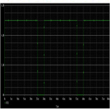
هدف از ارائه این مقاله طراحی و شبیه سازی گیت AND هشت ورودی در منطق CMOS میباشد. پیاده سازی یک مدار مجتمع در طی مراحل مختلفی انجام میگیرد. بدست آوردن چینش مدار یکی از مراحل بسیار مهم حساب میشود. در این پژوهش ابتدا در سطح چینش از نرم افزار LEDIT سپس برای شبیه سازی توصیف مدار طراحی شده در LEDIT به صورت یک نت لیست استخراج و این نت لیست به عنوان ورودی نرم افزار شبیه سازی PSPICE مورد استفاده قرار گرفته است. نتایج حاصل از شبیه سازی بیانگر عملکرد خوب مدار میباشد.
مقدمه
مکمل اکسید فلز نیمه هادی (CMOS) یک تکنولوژی برای ساخت مدارات مجتمع است. تکنولوژی CMOS در ریزپردازنده ها میکروکنترلرها ، RAM های استاتیک و دیگر مدارهای دیجیتالی استفاده می شود. تکنولوژی COMS برای برخی مدارات آنالوگ مانند سنسورهای تصویر ، مبدل های داده و فرستنده- گیرنده ی یکپارچه برای بسیاری از انواع ارتباطات نیز استفاده می شود. دو ویژگی مهم دستگاه های COMS عدم تصویر نویز و مصرف کم توان استاتیک می باشد. این منطق از دو قسمت شبکه بالابر و شبکه پایین بر تشکیل شده است. شبکه بالابر از ترانزیستورهای اثر میدان نوع P و شبکه پایین بر ااز ترانزیستورهای اثر میدان نوع N استفاده می کند. به مدار های AND, OR,NOT گیت های منطقی می گویند.
ABSTRACT
The purpose of this paper is to design and simulate the gateway AND of the eight inputs in the CMOS logic. The implementation of an integrated circuit takes place at different stages. Getting the circuitry is one of the most important steps. In this research, at first, at the level of the arrangement, the LEDIT software was used to simulate the description of the designed circuit in LEDIT as a list note and this list of notes was used as input for the PSPICE simulation software. The simulation results indicate good circuit performance.
INTRODUCTION
Semiconductor Metal Oxide Supplement (CMOS) is a technology for building integrated circuits. CMOS technology is used in microprocessors, microcontrollers, static RAMs and other digital circuits. COMS technology is also used for some analog circuits, such as image sensors, data converters and integrated transmitter / receiver for many types of communication. Two important features of COMS devices are the lack of image noise and static low power consumption. This logic consists of two parts of the network of lift and the downstream network. The lift network uses transistors of the P type field and the low-voltage network for N-type field effect transistors. The orbits AND, OR, NOT are called logical gates.
Year: ۲۰۱۸
Publisher : ۶th National Conference on Computer Science and Information Technology
By : Iman Sohrabi Chafjeiri, Hamid Gholipour Golroudbari, Mehdi Hatif, Behzad Taghipour Mouzen
File Information: English Language/ 8 Page / size: 265 KB
Only site members can download free of charge after registering and adding to the cart
سال : ۱۳۹۷
ناشر : ششمین کنفرانس ملی علوم و مهندسی کامپیوتر و فناوری اطلاعات
کاری از : ایمان سهرابی چافجیري , حمید قلی پور گلرودباري ,مهدي هاتف,بهزاد تقیپور موذن
اطلاعات فایل : زبان فارسی / 8 صفحه / حجم : KB 265


نقد و بررسیها
هنوز بررسیای ثبت نشده است.