توضیحات
چکیده
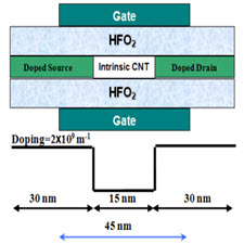
در اين مقاله با استفاده از روش شبيه سازی NEGFمشخصات انتقال ترانزيستورهاي اثرميداني نانولوله كربني كه مشابه ترانزيستورهاي ما سفت معمولي عمل ميكند مورد بررسي قرار خواهد گرفت. يكي از مشكلات اين گونه از ترانزيستورها، جريان نشتي حاصل از تونل زني حاملها در ولتاژهاي گيت-سورس منفي است. در اين مقاله ساختار اصلاح شده اي معرفي ميشود كه اثر قابل ملاحظه اي برروي كاهش اين جريان ناخواسته دارد. نتايج نشان ميدهد كه ساختار معرفي شده علي رغم سادگي، در محدوده ولتاژهاي موردنظر از مشخصات خاموشي بهتري بسيار برخوردار است .
مقدمه
با كاهش ابعاد ترانزيستورهاي ماسفت متعارف سيليكوني و مشكلات حاصل از اين كوچكسازي كه امكان ساخت يك ترانزيستور سيليكوني با مشخصات مطلوب را در اين ابعاد به چالش كشيده ها ، گزينه ي ديگري به عنوان جايگزين سيليكون به منظور استفاده در كانال ترانزيستورها معرفي شده اند نانوله ها كه يكي از اين گزينه نانولوله های کربنی می باشد. نانولوله هاي كربني به دليل امكان ساخت و استحكام لازم در قطر حدود نانومتر و طول حدود ميكرومتر، قابليت انتقال تقريبا بالستيك حاملها و امكان عملكرد هم به عنوان فلز و هم نيمه هادي با شكاف باند متفاوت توجه بسياري را به منظور استفاده در ساخت افزاره هاي الكترونيكي به خود جلب نموده است. تاكنون ساختارهاي متفاوتي براي اين نوع ترانزيستورها معرفي شده كه عمدتا ميتوان آنها را در سه گروه اصلي تقسيم بندی نمود. دسته اول كه ترانزيستور شاتكي(-SB CNTFET) شده ناميده اند با استفاده از اتصال دو كنتاكت فلزي به یک نانولوله کربنی ذاتی ساخته می شوند.
ABSTRACT
In this paper, using the NEGF simulation method, the transmission properties of transistors of carbon nanotubes that are similar to those of conventional rigid transistors will be investigated. One of the problems with this type of transistor is the leakage current generated by the carrier tunnel in the gate-source voltage is negative. In this paper, a modified structure is introduced which has a significant effect on the reduction of this unwanted flow. The results show that the proposed structure, despite the simplicity, has a better offset characteristics in the range of the desired voltages.
INTRODUCTION
By reducing the dimensions of the conventional silicon MOSFET transistors and the problems caused by this reduction, which made it possible to create an optimal silicon transistor in these dimensions, another option has been introduced as a silicon substitute for use in the transistor channel. One of these options is carbon nanotubes. Due to the possibility of fabrication of carbon nanotubes in a diameter of about nanometer and a length of about micrometer, the possibility of almost ballistic transmission of the carriers and the possibility of both metal and semiconductor performance with different bond gaps are of great interest for use in the manufacture of electronic devices Has attracted itself. Different structures have been introduced for this kind of transistors, which can be mainly divided into three main groups. The first group, called the SB-CNTFET transistor, is constructed using a compound of two metal contacts to an intrinsic carbon nanotube.
Year: 2010
Publisher : Eighteenth International Energy Conference of Iran
By : Reza Yousefi, Kamyar Saghafi, Kazem Moravj Farshi
File Information: persian Language/ 5 Page / size: 634 KB
سال :1389
ناشر : هجدهمین کنفرانس بین المللی برق ایران
کاری از : رضا يوسفي ,كاميار ثقفي, كاظم مروج فرشي
اطلاعات فایل : زبان فارسی / 5 صفحه / حجم : KB 634
![The Electricity Situation in Ghana[taliem.ir]](http://taliem.ir/wp-content/uploads/The-Electricity-Situation-in-Ghanataliem.ir_.jpg)


نقد و بررسیها
هنوز بررسیای ثبت نشده است.