توضیحات
چکیده
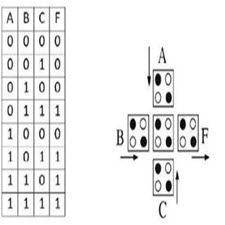
امروزه امکان کوچک تر کردن ترانزیستورها و تعبیه تعداد بیشتری از آن ها بر روی یک تراشه های سیلیکونی با محدودیت مواجه شده است به این منظور محققان به دنبال جایگزین های مناسبی برای آن هستند که مدارهای آتوماتای سلولی کوانتومی برای طراحی مدارهای دیجیتال، یکی از آن ها است. تمام جمع کننده ها یکی از بلوک های ساختمانی در مدارهای دیجیتال می باشد و به عنوان اصلی ترین واحد در مدارهای منطقی و محاسباتی دیجیتال محسوب می گردد. لذا بهبود عملکرد تمام جمع کننده ها ، تاثیر بسزایی در بهبود پارامترهای خروجی مدارات دیجیتال خواهد داشت. در این مقاله یک تمام جمع کننده بهینه ارایه گردیده است . نتایج شبیه سازی این تمام جمع کننده با استفاده از نرم افزار QCADesigner در مقایسه با سایر تمام جمع کننده ها اگر چه طرح پیشنهادی تعداد سلول های بیشتری دارد ولی در مقایسه دارای تاثیر کمتری بوده و طراحی آن ها تنها در یک لایه صورت می گیرد. و لایه های کمتر منجر به هزینه های کمتر خواهد شد.
مقدمه
در چند دهه اخیر مجتمع سازی نمایی در اندازه و همچنین در قابلیت افزایش توان پردازش به وسیله فناوری VLSI مبتنی بر لیتوگرافی معمولی بدست آمده است. با این حال با توجه به محدودیت های فیزیکی بنیادی فناوری CMOS مانند اکسیدهای گیت فوق العاده نازک, اثرات کانال کوتاه و لیتوگرافی این روند به طور فزایندهای با چالش های جدی مانند لیتوگرافی پرهزینه در مقیاس نانو مواجهه است بنابراین برای رشد صنعت الکترونیک باید به فکر فناوری های جایگزین بود به طوری که مشکلات گذشته زا حل کرده و توجیه اقتصادی داشته باشد و این فناوری نانو بود که نانو الکترونیک بنا نهاده شد.
ABSTRACT
Today, it is possible to minimize the transistors and embed more of them on a silicon chip. Consequently, researchers are looking for suitable alternatives for quantum cellular atomic circuits for designing digital circuits, one of them Is. All collectors are one of the building blocks in digital circuits and are considered as the main unit in digital rational and computational circuits. Therefore, improving the performance of all collectors will have a significant effect on the improvement of the output parameters of digital circuits. In this paper, an optimal collector is presented. The simulation results of this aggregator using QCADesigner software compared to all other collectors Although the proposed design has more number of cells, the comparison has less effect and their design is only in one layer. Lower layers will result in lower costs.
INTRODUCTION
In the last few decades, the integration of the size and also the ability to increase processing power by conventional VLSI technology has been achieved. However, due to the fundamental limitations of CMOS technology such as ultra-thin oxide, the effects of the short channel and lithography of this process are increasingly faced with serious challenges such as costly lithography on a nanoscale scale. Therefore, for the growth of the electronic industry, The alternative was to solve the past problems and have economic justification, and this nanotechnology was the basis of nanotechnology.
Year: 2017
Publisher : Second International Conference on Electrical Engineering, Computer Science and Information Technology
By : Vijayullah Parsaei
File Information: Persian Language/ 9 Page / size: 640 KB
Only site members can download free of charge after registering and adding to the cart
سال : 1395
ناشر : دومین همایش بین المللی مهندسی برق،علوم کامپیوتر و فناوری اطلاعات
کاری از : وجیه اله پارسایی
اطلاعات فایل : زبان فارسی / 9 صفحه / حجم : KB 640


نقد و بررسیها
هنوز بررسیای ثبت نشده است.